Printed Circuit board is a thin laminate sheet made up of fiberglass generally but also composite epoxy at times. It mechanically supports and electrically connects conducting material and electronic components.
PCB Composition
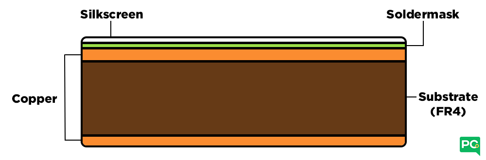
- Base – PCB is a thin laminate sheet made up of fibreglass (FR4) as its base material or substrate. This solid core gives the PCB its rigidity and thickness. It mechanically supports and electrically connects conducting material and electronic components. Cheaper PCBs and perf boards are made with other materials such as epoxies or phenolics which lack the durability of fibreglass but are much less expensive.
- Copper – Conducting material is mostly copper just like our traditional wires but a much miniature and embedded version of it running throughout the lengths and breaths of the PCB. It’s just like the veins in our body. The electronic components usually found sitting across the PCB are capacitors, resistors, translators and diodes. It’s just like the organs in our body. The copper layer is laminated to the board with heat and adhesive next to the base material. PCBs may have copper layers only on one side or both, further the number of copper layers can go on to 20 or more depending on the requirement.
- Wondering why copper?
- Its due to its high electrical conductivity and easy availability at low cost in comparison to other high conducting materials like silver or gold.
- Solder mask – The layer on top of the copper foil is called the solder mask layer. It protects the PCB surface and insulates the copper circuit from oxidation from the environment, accidental contact with other metal, solder or conductive bits. It gives the green or other desired colour to the board, however solder mask is applied in such a way that it cover up the small traces but leaves the silver rings and SMD (Surface Mount Device) pads exposed so they can be soldered to. It also makes the PCB high temperature resistant. A solder mask is nothing but a layer of polymer.
- Silkscreen – On top of solder mask, a white layer of silkscreen is applied. It is used for nomenclature on the board by adding letters, symbols and numbers to the PCB that makes assembly and working convenient.
- Mounting – Once the layers are stacked just like a lasagne, various mountings are made on the board, so it can interact with different boards or with different components within the board.
- Annular rings – gold/nickel plated around the holes on the board.
- Finger – exposed metal pads along the edge of the board, used to create a connection between two circuit boards.
- Via – a hole in a board used to pass signal from one board to another.
- Electronic Components – Few of the electronic components generally used are as follows:
- SMD / SMT – (Surface Mount Device / Surface Mount Technology) These are tiny components which are placed on one side of the PCB and do not affect the components on the other side. Smaller footprint and easy to mount on PCB using robots and machines.
- THT – (Through Hole Technology) These are components with long leads which pass from one side of the PCB to the other side, which can be advantages or disadvantages depending on the design. But it takes larger footprint and difficult to mount these components on PCB using machines and robots.