This knowledge base article provides a detailed explanation and example for initializing GPIO pins on the STM32F407VE microcontroller by directly manipulating hardware registers via their addresses. This is fundamental for embedded C developers who require low-level control over the hardware for custom applications.
Overview:
The STM32F407VE microcontroller from STMicroelectronics features multiple general-purpose input/output (GPIO) ports having two 32-bit configuration registers, two 32-bit data registers, a 32-bit set/reset register, a 16-bit reset register, and a 32-bit locking register, each GPIO port is controlled using a set of memory mapped registers, by writing the code, can able to set the GPIO port pin mode as OUTPUT, then the speed and internal pull-up/ pull-down resistors and also by using the address enable the clocks for the peripheral. Understanding how to initialize and control the GPIO pins at the register level enables us to create highly efficient and tailored embedded systems.
Key steps for GPIO pin initialization:
1. Enable the GPIO Clock:
Before configuring GPIO pins, the corresponding GPIO port’s clock must be enabled in the RCC (Reset and Clock Control) register.
Register: RCC_AHB1ENR (AHB1 Peripheral Clock Enable Register)
Action: Set the bit corresponding to the GPIO port (e.g., GPIOAEN for GPIOA).
- RCC->AHB1ENR |= (1 << 0); // Enable GPIOA clock (bit 0 for GPIOA)
2. Configure the GPIO Pin Mode
The GPIO pin mode is configured in the GPIOx_MODER register. Each pin has two bits to define its mode:
00: Input
01: General-purpose output
10: Alternate function
11: Analog
Register: GPIOx_MODER (GPIO Port Mode Register)
Action: Set the appropriate bits for the desired pin.
- GPIOA->MODER &= ~ (3 << (2 * 5)); // Clear mode bits for PA5
- GPIOA->MODER |= (1 << (2 * 5)); // Set PA5 as output (01)
3. Configure Output Type (if applicable)
For output mode, configure the output type in the GPIOx_OTYPER register:
0: Push-pull
1: Open drain
Register: GPIOx_OTYPER (GPIO Port Output Type Register)
Action: Set or clear the bit for the desired pin.
- GPIOA->OTYPER &= ~ (1 << 5); // Set PA5 as push-pull
4. Configure Output Speed
The output speed is set in the GPIOx_OSPEEDR register:
00: Low speed
01: Medium speed
10: High speed
11: Very high speed
Register: GPIOx_OSPEEDR (GPIO Port Output Speed Register)
Action: Set the appropriate bits for the desired pin.
- GPIOA->OSPEEDR |= (2 << (2 * 5)); // Set PA5 to high speed (10)
5. Configure Pull-Up/Pull-Down Resistors
The pull-up/pull-down configuration is set in the GPIOx_PUPDR register:
00: No pull-up/pull-down
01: Pull-up
10: Pull-down
Register: GPIOx_PUPDR(GPIO Port Pull-Up/Pull-Down Register)
Action: Set the appropriate bits for the desired pin.
- GPIOA->PUPDR &= ~ (3 << (2 * 5)); // Clear pull-up/pull-down bits for PA5
- GPIOA->PUPDR |= (1 << (2 * 5)); // Enable pull-up for PA5 (01)
6. Configure Alternate Function (if applicable)
If the pin is used for an alternate function (e.g., UART, SPI), configure the GPIOx_AFRL or GPIOx_AFRH register. Each pin has 4 bits to select the alternate function.
Register: GPIOx_AFRL (for pins 0–7) or GPIOx_AFRH (for pins 8–15)
Action: Set the appropriate bits for the desired pin.
- GPIOA->AFR [0] &= ~ (0xF << (4 * 5)); // Clear alternate function bits for PA5
- GPIOA->AFR [0] |= (0x1 << (4 * 5)); // Set PA5 to AF1 (e.g., TIM2_CH1)
7. Write to the Pin (if Output Mode)
To set or reset the pin, use the GPIOx_BSRR register:
Set: Write 1 to the lower 16 bits.
Reset: Write 1 to the upper 16 bits.
- GPIOA->BSRR = (1 << 5); // Set PA5
- GPIOA->BSRR = (1 << (5 + 16)); // Reset PA5
Register Map Reference:
RCC->AHB1ENR (0x40023830): Controls clock gating for GPIO ports. Example: Bit 0 enables GPIOA clock.
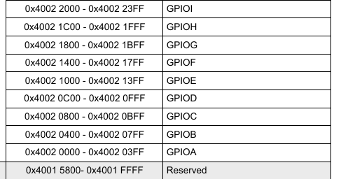
GPIOx->MODER (0x40020000 + offset): Selects mode of pins (2 bits per pin).
GPIOx->OTYPER: Configures output type for each pin (1 bit per pin).
GPIOx->OSPEEDR: Selects output speed for each pin (2 bits per pin).
GPIOx->PUPDR: Configures pull-up/pull-down resistors for each pin (2 bits per pin).
Note: x is the GPIO port letter (A, B, C, etc.)
Practical Example: Initialize PA5 as Push-Pull Output:
This example shows how to initialize pin 5 of GPIO port A (PA5) as a push-pull output at medium speed with no pull-up or pull-down resistors. This is commonly used to control an LED connected to that pin.
code:
#include "stm32f4xx.h"

void GPIO_Init(void) {
    // Step 1: Enable clock for GPIOA
    RCC->AHB1ENR |= RCC_AHB1ENR_GPIOAEN;

    // Step 2: Set PA5 mode to output (01)
    GPIOA->MODER &= ~(0x3 << (5 * 2));   // Clear bits for PA5
    GPIOA->MODER |=  (0x1 << (5 * 2));   // Set PA5 as output

    // Step 3: Set output type to push-pull (0)
    GPIOA->OTYPER &= ~(0x1 << 5);

    // Step 4: Set output speed to medium (01)
    GPIOA->OSPEEDR &= ~(0x3 << (5 * 2)); // Clear bits for PA5
    GPIOA->OSPEEDR |=  (0x1 << (5 * 2)); // Medium speed

    // Step 5: No pull-up/pull-down (00)
    GPIOA->PUPDR &= ~(0x3 << (5 * 2));
}

int main(void) {
    GPIO_Init();

    while (1) {
        // Toggle PA5 output state
        GPIOA->ODR ^= (1 << 5);
        for (volatile int i = 0; i < 100000; i++); // Delay
    }
}
Important Notes:
Always enable the GPIO peripheral clock before configuring the registers, or the settings will have no effect.
Bit manipulations use shifts and masks to target specific pin configuration bits within registers.
Use the official STM32F4 reference manual and datasheet for detailed register maps and descriptions.
This example assumes the stm32f4xx.h CMSIS header is included for register definitions.
conclusion:
Direct register programming for GPIO initialization on the STM32F407VE requires enabling peripheral clocks and configuring the multiple registers that control pin behavior. Mastery of these steps provides efficient, reliable hardware control essential for embedded development.