Overview
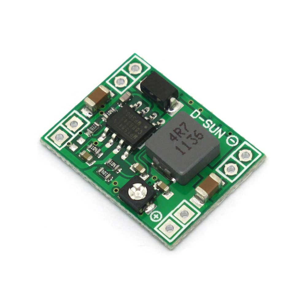
- Product Name: eBoot Mini MP1584EN DC-DC Buck Converter
- Manufacturer: Based on Monolithic Power Systems (MPS) MP1584EN chip
- Type: Synchronous buck (step-down) DC-DC converter module
- Primary Use: Voltage regulation in electronics projects, prototyping, and low-power applications
- Typical Price Range: $4–$10 USD (varies by seller)
- Availability: Online retailers like Amazon, eBay, AliExpress, or eBoot direct
- Datasheet Reference: MP1584EN datasheet from MPS (search for “MP1584EN datasheet” for full technical details)
Key Specifications
- Input Voltage Range: 4.5V to 28V DC (absolute max 30V; recommended 5V–24V for stability)
- Output Voltage Range: Adjustable 0.8V to 18V (via onboard 10kΩ potentiometer)
- Output Current: 3A continuous (4A peak); derates to 2A at >50°C ambient
- Efficiency: 85–95% (optimal at moderate loads and voltage differentials)
- Switching Frequency: ~1.5 MHz
- Quiescent Current: ~0.5mA
- Ripple Voltage: <100mV (at 1A load; can be reduced with external caps)
- Dimensions: 22mm x 17mm x 4mm
- Weight: ~5g
- Operating Temperature: -40°C to +85°C
- Protections: Over-current (OCP), over-temperature (OTP), short-circuit; no reverse polarity protection
Features and Components
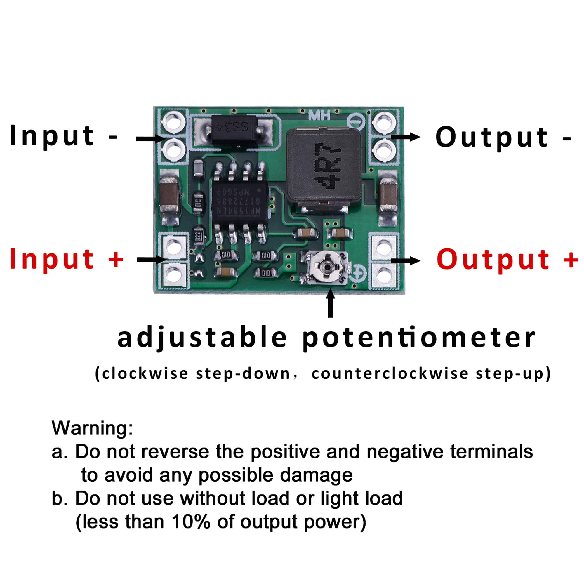
- Adjustability: Onboard potentiometer for easy voltage tuning; can be replaced with fixed resistors for precision (Vout = 0.8V * (1 + R2/R1))
- Indicators: Power-on LED
- Internal Design: Synchronous buck topology with integrated MOSFETs, 22µH inductor, and capacitors
- Pinout:
- VIN+: Input positive
- VIN-: Input ground
- VOUT+: Output positive
- VOUT-: Output ground
- ADJ: Adjustment pin
- EN: Enable pin (pull low to disable)
- Form Factor: Miniature, breadboard-friendly with screw terminals
How It Works
The Mini MP1584EN is a synchronous buck converter, a type of DC-DC switching regulator that efficiently steps down (reduces) a higher input DC voltage to a lower, stable output DC voltage. It uses high frequency switching to achieve this, based on the MP1584EN integrated circuit (IC) from Monolithic Power Systems. Below, I’ll break down its operation step-by-step, including the underlying buck topology, internal mechanisms, and practical considerations. This explanation draws from standard power electronics principles and the MP1584EN datasheet.
Basic Buck Converter Concept
- What It Does: A buck converter “bucks” (reduces) the input voltage (Vin) to a lower output voltage (Vout). For example, it can take 12V from a battery and output 5V for a device.
- Key Components in a Buck Circuit:
- Switch (MOSFET): Turns on/off rapidly to control energy flow.
- Inductor (L): Stores and releases energy as magnetic flux.
- Capacitor (C): Smooths the output voltage by storing charge.
- Diode or Second MOSFET: In synchronous designs, a second MOSFET replaces the diode for better efficiency.
- Feedback Loop: Monitors output and adjusts the switch duty cycle.
- Analogy: Think of it like a water pump: The switch opens/closes a valve to fill a tank (inductor) with water (energy) at high pressure (Vin), then releases it at lower pressure (Vout) through a smoothing reservoir (capacitor).
The output voltage is approximately Vout = Vin × Duty Cycle (D), where D is the fraction of time the switch is on (0 < D < 1). For stability, D adjusts automatically via feedback.
How the MP1584EN Specifically Works
- Topology: Synchronous buck (uses two MOSFETs: high-side for switching low-side for rectification). This differs from non-synchronous bucks that use a diode, which wastes energy as heat.
- Switching Process (Step-by-Step Cycle at ~1.5 MHz Frequency):
- On Phase (Switch Closed): The high-side MOSFET turns on, connecting Vin to the inductor. Current ramps up in the inductor, storing energy. The low-side MOSFET is off. Energy flows from Vin through the inductor to the load and capacitor.
- Off Phase (Switch Open): The high-side MOSFET turns off, and the low-side MOSFET turns on. The inductor’s magnetic field collapses, releasing stored energy as current continues flowing through the low-side MOSFET to the output. This maintains voltage across the load.
- Cycle Repeats: The process loops rapidly (1.5 million times per second), averaging the voltage to a steady Vout.
- Duty Cycle Control: The MP1584EN’s internal error amplifier compares Vout (via a voltage divider) to a reference (set by the potentiometer, e.g., 0.8V internal reference). If Vout is low, it increases D; if high, it decreases D. This is pulse-width modulation (PWM).
- Waveforms (Simplified Text Representation):
- Switch Voltage: Square wave (high during on-phase, low during off-phase).
- Inductor Current: Triangular ramp (up during on, down during off).
- Output Voltage: Nearly flat DC with small ripple (filtered by capacitor).
- Efficiency Boost: Synchronous design reduces conduction losses (diode drop ~0.7V vs. MOSFET ~0.1V), achieving 85–95% efficiency. At light loads, it enters pulse-frequency modulation (PFM) to save power.
Internal Block Diagram and Key IC Features
- MP1584EN IC Overview: A monolithic IC with integrated 28V MOSFETs, oscillator, comparator, and protections. It handles up to 3A output.
- Block Diagram (Conceptual):
- Input → High-Side MOSFET → Inductor → Output Capacitor → Load.
- Feedback: Output voltage sensed and fed back to error amp, which controls the PWM generator.
- Enable Pin: Allows external on/off control (e.g., for power saving).
- Adjustability: The potentiometer forms a resistor divider that sets the feedback voltage. Vout = 0.8V × (1 + R_adj / R_fixed), where R_adj is the pot’s variable resistance.
Practical Operation and Considerations
- Startup and Stability: On power-up, the IC soft-starts to avoid inrush current. The output capacitor (typically 100µF) ensures stability; without it, ripple increases.
- Load Response: Handles varying loads well due to fast switching, but heavy loads (>3A) cause voltage droop or heating.
- Limitations: Buck-only (can’t increase voltage); non-isolated (input/output grounds connected); EMI from switching (mitigate with filters).
- Efficiency Factors: Peaks at 50–80% load; drops at extremes due to switching losses or quiescent draw.
- Testing Tip: Use an oscilloscope to view switching waveforms or a multimeter for Vout. For simulation, tools like LTspice can model it.
Applications
- Powering microcontrollers (e.g., Arduino, Raspberry Pi) from batteries or adapters
- LED drivers and lighting systems
- Battery charging circuits (with BMS)
- Robotics, drones, and automotive electronics
- IoT devices and portable gadgets
Pros and Cons
- Pros:
- High efficiency and compact size
- Built-in protections and easy adjustment
- Low cost and no-soldering setup for basics
- Cons:
- No isolation (risk of ground loops)
- Buck-only (no boost capability)
- Potentiometer drift over time
- Heat buildup at high loads without cooling
Usage Tips and Safety
- Setup: Connect input, adjust voltage unloaded, then apply load. Use multimeter for verification.
- Heat Management: Add heatsink or ensure airflow for >1A loads.
- Enhancements: Add 10µF output capacitor for stability; use LC filters for noise reduction.
- Safety Precautions: Avoid input >28V; protect against reverse polarity; not waterproof—enclose for outdoor use.
Troubleshooting
- No Output: Check input voltage (>4.5V), enable pin, or shorts.
- Unstable Voltage: Add capacitors or check load.
- Overheating: Reduce current or improve ventilation.
- Noise/EMI: Add ferrite beads or shielding.